Laptop computer designers, audio amplifier makers, and power supply manufacturers can keep their products cooler by following these fundamental heat-sink design equations for natural convection and forced-air cooling.

Power transistors and modules, many power-supply regulator assemblies, and high-current diodes typically generate more heat than their own mass can safely dissipate. For this reason, power devices must securely fasten to a suitable heat sink to effectively increase the mass and surface area of their heat-dissipating junctions. Heat sinks come in a wide variety of shapes, sizes, colors, and surface finishes for specific and general applications for semiconductor circuitry.
Power device heating
The amount of heat that a power semiconductor or module generates depends upon its mode of operation, bias level, signal amplitude, and the shape of the applied signal. For example, power transistors used as Class A amplifiers for sine or complex waves or pass transistors and modules for regulating dc power supplies generate much more heat than square-wave oscillators, Class AB amplifiers, Class B square-wave amplifiers, and PWM (pulse width modulation) amplifiers. For example, when a power transistor operates with square waves, the collector voltage is high with low current, then high current with low voltage during the saturation and cutoff periods. The result is very low average power dissipation. But, in either case, these devices need some type of heat sink to help dissipate the internal power they generate.
Thermal gradient and temperature differential
A silicon power transistor or high-current diode that must be heat sinked has an allowable maximum junction temperature of usually 150 °C or a little more. If the heat-generating device does not connect to a greater mass or surface area, the amount of junction current and voltage as given in a typical specification sheet could hardly be approached before the device would exceed the maximum collector junction temperature. The reason is that the device specification sheets list their characteristics with the device mounted on a heat sink of considerable size, usually called an “infinite” heat sink.
The temperature of the air surrounding the heat-generating device must be much less than the maximum allowable junction temperature for the device to cool. The heat sink attempts to reduce the junction temperature to that of the surrounding medium. If the heat sink was thermally perfect, the transistor junction temperature could reach the same as the lower ambient. However, this is not possible in practice. The thermal conductivity path from the transistor junction to the ambient air contains physical connections between the junction and case, case and heat sink (through an insulator, if used), and heat sink and ambient. These connections are not thermally perfect and therefore produce a temperature differential. They are thermal resistances, and each thermal resistance has a unique coefficient number. The coefficient is expressed as a temperature in degrees centigrade per watt of dissipation (°C/W). Due to these resistances, a temperature differential always appears between the collector junction and ambient. This variable must be kept to a minimum.
The actual temperature difference depends upon the amount of power the junction dissipates. The average power dissipation for a transistor is approximately: Pd=Ic x Vce , where Pd = power dissipation in watts of constant current generation; Ic = collector current; and Vce = collector-to-emitter voltage.
First, study the characteristics of a single-ended, class A amplifier stage. The transistor selected for this example has a peak collector current of 15 A and a power dissipation capability of 90 W at a case temperature of 25°C. The power dissipation capability decreases linearly from 25°C to zero watts of dissipation at 100 °C case temperature. See Figure 1.

Transistor specifications for power dissipation are typically rated at 25 °C and derated to zero at 100 °C. The variables for a reliable design must fall under the curve.
When the Class A amplifier stage output power is 90 W peak, the quiescent collector current is about 1.5 A at 30 V collector-to-emitter (biased at midpoint on its load line). Using the equation for power dissipation, the class A stage produces 45 W (Pd = 30 V x 1.5 A = 45 W). The product of collector current and voltage either side of this quiescent state produces less power dissipation, so 45 W is the maximum power dissipation to consider. This value is used below to calculate the heat sink required.
Heat sink characteristics
A suitable heat sink can now be selected. As the amount of power dissipation in the device increases, the size of the heat sink must increase to allow more surface area to be exposed to the ambient. First, the heat sink material and size are considered. Thermal conductivity of the material should be as high as possible. Copper is about the best for thermal conductivity and aluminum follows a close second. The difference in cost between copper and aluminum exceeds their difference in thermal conductivity, therefore aluminum heat sinks are pretty much an industry standard. The ability of aluminum to conduct heat to the ambient is measured in °C/W of power dissipation, which primarily depends on its surface area and finish.
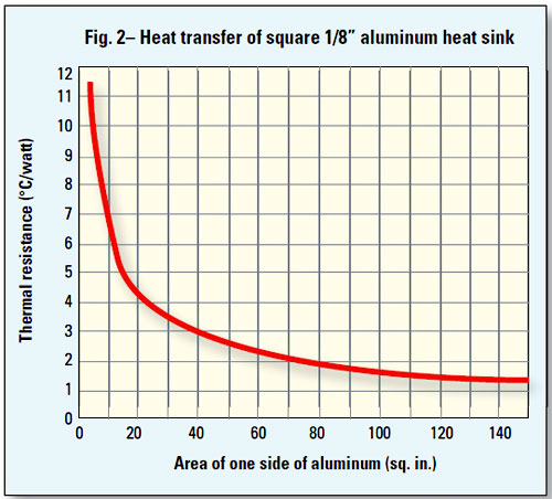
First, consider a square of bright aluminum, 1/8-in. thick with a surface area of 5 in.2 per side, positioned vertically. From actual measurements, the thermal resistance is about 9 °C/W. Refer to Figure 2. If it increases to 10 in.2, the thermal resistance reduces even more until a practical limit is reached of about 140 in.2 of heat sink area. Here, the thermal resistance is about 1.4 °C/W in free air, and increasing the surface area does not significantly decrease the thermal resistance. More than 140 in.2 in this case would be considered an infinite heat sink. Copper positioned vertically, 1/8-in. thick, by 140 in.2 has a thermal resistance of about 1.0 °C/W compared to aluminum at 1.4 °C/W.

The thermal resistance drops rapidly from no heat sink to 3.0 °C/W at 40 in.2 and levels off to about 1.5 °C/W as the heat sink size reaches about 100 in.2 (infinite heat sink). Increasing it any further makes little difference.
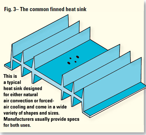
The most commonly used type of commercially available heat sink is the finned extruded aluminum style, as shown in Figure 3. It is usually painted flat black with a bare exposed area for mounting the semiconductor device, or it may be completely black anodized. It can be punched to accommodate any pin or mounting arrangement. This basic shape of radiator is most desirable for forced air and natural convection cooling because much surface area is exposed to the surrounding air within a comparatively small volume. Approximately 80 in.2 of radiating surface can be contained in a volume of only 4.5 x 1.5 x 3 in. These same heat sinks can be given a serrated surface to increase even more the available surface area per unit volume. Also, some heat sinks come in “pin-grid arrays” and other geometries for special applications.

This is a typical heat sink designed for either natural air convection or forced-air cooling and comes in a wide variety of shapes and sizes. Manufacturers usually provide specs for both uses.
Now, return to the sample calculations for heat dissipation and match the requirements to a proper heat sink. First, sum the thermal resistances, multiply the sum by the power dissipation of the semiconductor, and add the results to the ambient temperature. This yields a new junction temperature. If the temperature just calculated exceeds the maximum allowable temperature for the device as shown in the derating curve (Figure 1), one or more factors in the computation must be changed. For example, the ambient temperature could be lowered or the power dissipation reduced by lowering the input voltage or current. Also, any one of the thermal resistances could be reduced to achieve the same end.

For the steady state case, this is the thermal circuit that is equivalent to Kirchoff’s law for an electrical circuit.
Refer to Figure 4: The equation used for determining the device junction temperature is:
Tj = Pd(Θjc + Θcs + Θsa) + Ta, and
Θja = Θjc + Θcs + Θsa, or
Tj = Pd (Θja) + Ta
where:
Tj = junction temperature, °C
Pd = power dissipation, W
Θjc = junction thermal resistance, °C/W
Θcs = insulator thermal resistance, °C/W
Θsa = heat sink thermal resistance, °C/W
Θja = junction to ambient, °C/W
Ta = ambient temperature, °C
The previous calculations of the single-ended, Class A amplifier dissipated 45 W. Select a maximum ambient temperature of 50 °C; a transistor thermal resistance Θjc of 0.8 °C/W; silicone grease to give a Θcs of 0.1 °C/W; and a commercial heat sink as shown in Figure 4 with a Θsa of 1.8 °C/W.
Now check it out:
Tj = 45(0.8 + 0.1 + 1.8) + 50
Tj = 171.5 °C
This is not a satisfactory solution: only a Tj of 98.6 °C is allowed in the example, so fine-tune the numbers in order to lower the temperature to a more reasonable level. Although this temperature is under the maximum allowable for the transistor, a look at the derating graph shows that only 2 W of dissipation is allowed at 98 °C. The transistor would have to dissipate 16 W more than it was designed to handle and would quickly fail. Lowering the ambient from 50 °C to 30 °C would yield a Tj of 78 °C and the derating curve allows over 18 W at this temperature, so this is a satisfactory heat sink, transistor, ambient temperature combination. However, if the original 50 °C is a necessary parameter, then reduce the required output power; use additional output stages; select a different power transistor (where Tj = 175 to 200 °C maximum) or heat sink (or use forced-air cooling as discussed below).

This is a convenient graph for quickly determining whether a particular heat sink will work without much calculation.
Heat Sink spec Sheets
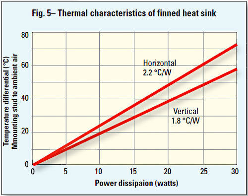
Graphs, charts, and tables supplied with fabricated heat sinks yield much useful information as to how they can be efficiently used. A typical graph as shown in Figure 5 conveys the thermal resistance characteristics for the heat sink in Figure 3. The temperature differential reads directly in °C from the mounting to ambient air as seen on the vertical axis of the graph. The power dissipation capability of the heat sink in watts is plotted along the horizontal. The vertically mounted heat sink has a thermal coefficient of about 2.2 °C/W. The transistor can be isolated electrically from the heat sink with a mica or other insulator. However, the mica insulator has a coefficient of 0.8 °C/W to 0.5 °C/W, which must be added to the thermal resistance of the heat sink. Silicone grease on both sides of the insulator reduces the resistance by half or 0.4 to 0.25 °C/W. In any case, the transistor or module should be mounted near the lower edge of a vertically mounted heat sink for best dissipation.
Another special characteristic some manufacturers indicate is the effect of forced airflow for a natural convection heat sink as shown in Figure 6. Thermal resistance of the heat sink is shown along the ordinate and the airflow in CFM is given along the abscissa. As shown, the thermal resistance of the heat sink can be reduced considerably from 1.7 to less than 0.6 °C/W with airflow of only 16 CFM.

A little forced-air flow makes a big difference in thermal resistance when space permits a fan or blower.
The ambient temperature of 30 °C that was decided upon as a solution for the amplifier stage is too low to be used in actual practice. A much more realistic temperature is the 50 °C that was first proposed. Using the 18 W previously calculated, select a forced airflow of 16 CFM, heat sink Θsa of 0.6 °C/W, and an ambient of 50 °C. Substitute these values in the equation for solving Tj, and the result is 77 °C. The derating curve shows an allowable 25 W at 77 °C, so forced air is indeed a viable option. However, this means that each transistor or power module requires its own heat sink with airflow of 16 CFM. The forced air cooling made the difference between an impossible and a possible circuit-heat sink combination for a 50 °C environment.

Do you want to know more?
Heat sink Design and Selection
Heat sink machining and finishing
What is an aluminum heat sink?


